Peter Lobner
On 8 July 2016, the Semiconductor Industry Association (SIA) and its international partners announced the release of the 2015 International Technology Roadmap for Semiconductors (ITRS), which it describes as follows:
ITRS is “a collaborative report that surveys the technological challenges and opportunities for the semiconductor industry through 2030. The ITRS seeks to identify future technical obstacles and shortfalls, so the industry and research community can collaborate effectively to overcome them and build the next generation of semiconductors – the enabling technology of modern electronics.”
 You can download the 2015 ITRS Executive Report and the seven technical sections at the following link:
http://www.semiconductors.org/main/2015_international_technology_roadmap_for_semiconductors_itrs/
Key points from the Executive Report are the following:
- Economic gains from adopting manufacturing processes and packaging for smaller transistors are decreasing.
- The magnitude of the investment needed for developing the processes and devices for manufacturing the highest performance chips has reduced the number of top-tier manufacturers (IC foundries) to just four.
- Advanced manufacturing technologies exist for increasing transistor density, including smaller 2D features and 3D (stacked) features.
- As features approach 10 nm (nanometers), the IC manufacturers are running out of horizontal space.
- Flash memory is leading the way in 3D manufacturing to enable higher packing densities.
- As packing densities continue to increase, new techniques will be needed by about 2024 to ensure adequate heat removal from the highest density chips.
- At some point, liquid cooling may be required.
- Companies without fabrication facilities (i.e., Apple) are producing the IC design, which is manufactured by a foundry company (i.e., Samsung manufactures the Apple A6X IC).
- A new “ecosystem” has evolved in the past decade that is changing the semiconductor industry and blurring the way that performance scaling is measured.
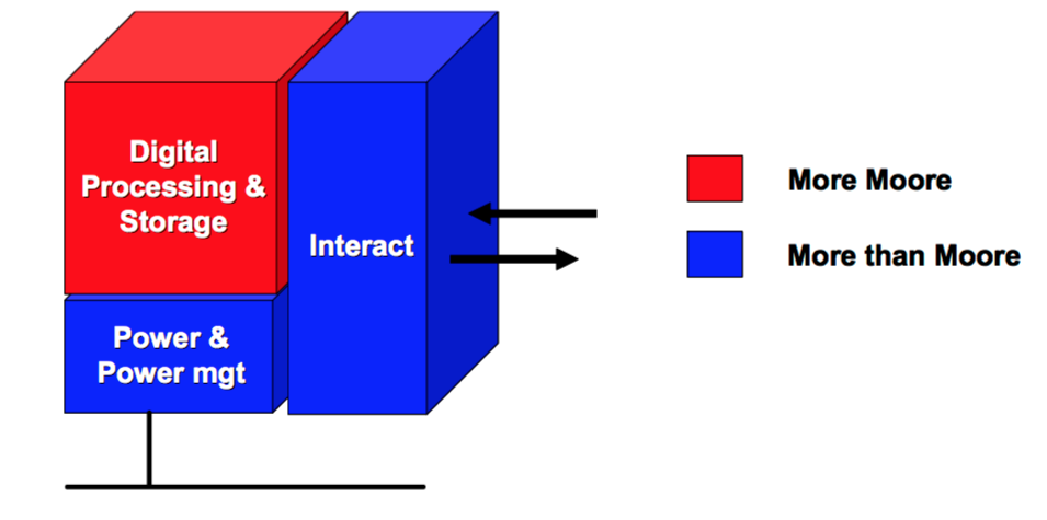
- Manufacturing advances enable further miniaturization of IC features and the integration of digital system functions (i.e., logic, memory, graphics, and other functionality) in a single die (system-on-a-chip, SOC). This is known as “More Moore” (MM).
- System integration and packaging advances enable multiple related devices (i.e., power & power management, interfaces with the outside world) to be integrated in a single package along with the IC (system-in-package, SIP). This is known as “More-than-Moore” (MtM).
- You can see the distinction between MM and MtM in the following diagram from the IRTS white paper, “More-then-Moore,” by Wolfgang Arden, et al., http://www.itrs2.net/uploads/4/9/7/7/49775221/irc-itrs-mtm-v2_3.pdf
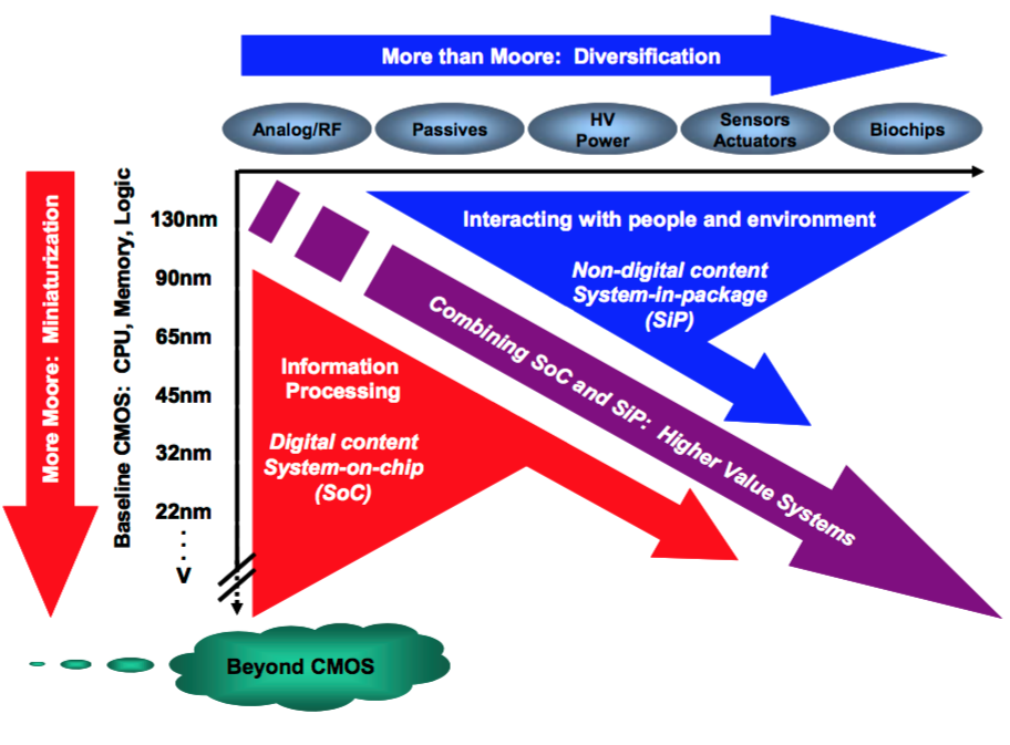
The transition to computationally intensive cloud computing enables effective use of “big data”. In contrast, there has been a proliferation of smart, low-power, functionally diverse devices that generate or use instant data, and can be linked to the cloud as part of the Internet of Things (IoT). These different ends of the spectrum (cloud & IoT) create very different demands on the semiconductor industry. They also complicate measurement of industry performance. It’s not just Moore’s Law anymore.

The 2015 IRTS offers an expanded set of metrics to assess the combined performance of SoC and SIP in delivering higher value systems. This measurement scheme is shown conceptually below (from the same IRTS “More-then-Moore” white paper cited above).
For another perspective on the 2015 ITRS report, you can read a short article by Sebastian Anthony on the arsTECHNICA website at the following link: